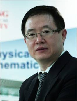
Keynote speaker's bio:
Professor Ze Xiang SHEN
Professor, Division of Physics and Applied Physics,
School of Physical and Mathematical Sciences;
School of Materials Science and Engineering;
Program Chair, Interdisciplinary Graduate School;
Director, Centre for Disruptive Photonic Technologies;
Major Research Interests: Near-field Raman microscopy, Graphene and 2D materials, Energy storage, Plasmonics
Nanyang Technology University, Singgapore.
Dr. Ze Xiang Shen is a Professor in the School of Physical and Mathematical Sciences, and the School of Materials Science and Engineering, Nanyang Technological University. He is Co-Director, Centre for Disruptive Photonics Technologies at NTU.
His main research areas include carbon related materials, especially graphene. His work involves spectroscopic and theoretical study of few-lay graphene and folded graphene, graphene intercalation study, graphene based composites for energy harvesting (Li Ion batteries and supercapacitors) and nano electronics; He also works on developing near-field Raman spectroscopy/imaging techniques and the study of plasmonics structures where some very fundamental questions remain to be answered.
Recently he has been active in the study of 2D materials and Perovskites using ultra Low wavenumber Raman spectroscopy, PL techniques and time resolved spectroscopy in combination with high pressure and low temperature.
He was awarded the NTU Nanyang Award for Research and Innovation 2009 as well as the Gold Medal for Research Excellence by Institute of Physics Singapore in 2011. Shen authored over 400 peer reviewed journal papers, 4 book chapters, edited 5 books and over 300 conference papers. He has a citation of >27,000 and H-index of 78.
Keynote speech title: Tuning2D Materials by Stacking Order for Energy Harvesting and Nanoelectronic Applications
Keynote speech abstract:
It is well-known that the optical and electronic structures of two-dimensional transition metal dichalcogenide (2D TMD) materials and perovskites often show very strong layer-dependent properties. It is less well-known however is that the properties can also be tuned by stacking order, which allows us to build electro and optical devices with the same material and the same thickness. Detailed understanding of the inter-layer interaction will help greatly in tailoring the properties of 2D TMD materialsfor applications, e.g. in pn junction, transistors, solar cells and LEDs. Raman/Photoluminescence (PL) spectroscopy and imaging have been extensively used in the study of nano-materials and nano-devices. They provide critical information for the characterization of the materials such as electronic structure, optical property, phonon structure, defects, doping and stacking sequence.
In this talk, we use Raman and PL techniques and electric measurements, as well as simulation to study 2- and 3-layer 2D TMD samples.The Raman and PL spectra also show clear correlation with layer-thickness and stacking sequence. Electrical experiments and ab initio calculations reveal that difference in the electronic structures mainly arises from competition between spin-orbit coupling and interlayer coupling in different structural configurations.
|